Current Research Areas
|
The focus of research of Aitchison Group is micro and nano fabrication for optical sensing and signal processing. This covers a broad range of research areas including nonlinear optics, plasmonics, silicon and III-V photonics. |
Portable cytometry for blood and cell analysisXilong Yuan (Google scholar) |
 CD4 cell counting for HIV monitoring Point of care testing (POCT) are widely needed for disease diagnosis such as HIV, infection and anemia. A blood cell/particle imaging platform has been developed using microfluidics to control sample motion. Fluorescent detection system and particle/cell counting algorithm are achieved. One prototype used for CD4 T cell counting has been developed for HIV/AIDS disease monitoring and it demonstrated the feasibility and great potential of the system in limited healthcare settings. Key words: cytometer, microfluidics, fluorescence, CD4  Multiplex bead assay and detection for dengue fever Microspheres labelled with multiple dyes can be used to perform high-throughput multiplexing assays. Based on a similar principle as flow cytometry, a microfluidic imaging platform is being developed into a smaller form factor and it generates quantitative data of biomarkers from the captured images. We seek to demonstrate the detection of multiple dengue fever biomarkers via a custom designed optics. To achieve the detection objective, we are interested in electromagnetic focusing and acoustic focusing in the imaging channel. Microfluidic designs can be simulated in multiphysics tools and fabricated for experimental testing. The detection of fluorescent bead requires a uniform light source to excite the fluorophores. We have demonstrated strategies of using non-collimated and collimated source to improve the uniformity of the fluorescence illumination. Additionally, imaging processing algorithms are being developed, such as region recognition, intensity classification, thresholding and calibration. Key words: multiplexing assay, biomarkers, fluorescent probes, biosensors, optics, microscope, laser, LED, filters, image processing, machine learning . |
Plasmonic AlGaAs Waveguides for Four Wave MixingKyle Johnson |
|
Plasmonic waveguides can be used to concentrate light below the diffraction limit, increasing the optical intensity inside the waveguide. This effect can be utilized to greatly enhance nonlinear processes such as four wave mixing (FWM), allowing the creation of nonlinear devices with very small dimensions. Our research is focused on investigating the use of plasmonic waveguides with an AlGaAs core to create efficient FWM devices with potential applications for optical signal processing, such as signal regeneration and wavelength conversion.
Key words: Nonlinear Optics, Plasmonics, Integrated Optics . |
Vertical integration approach in AlGaAsZhongfa Liao (Google scholar) |
 Many of the basic material properties of AlGaAs/GaAs are advantageous to designing photonic integrated circuits (PICs). All compositions of AlxGa1-xAs are lattice matched. The band gap energy can be varied from 1.42 eV (GaAs) to 2.17 eV (AlAs) and, similarly, the index of refraction at 850 nm can be varied from 3.68 (GaAs) to 2.99 (AlAs). These make epitaxy processes less restrictive and offer more design flexibility. The 785 - 850 nm spectral window has several potential applications. For non-invasive bio sensing, it is the wavelength range where hemoglobin has the lowest absorption. As current data center communication systems use 850 nm vertical cavity lasers, monolithic integration would enable efficient wavelength division multiplexing devices. AlGaAs/GaAs has also been identified as the promising material system for quantum optics. The integration of pump lasers, nonlinear optical elements and signal processing waveguides opens the possibility of a true quantum optics technology. |
Nonlinear optics in semiconductor superlatticesPisek Kultavewuti |
Our group works on nonlinear optics in
semiconductors and superlattices, especially
an AlGaAs system which possesses highly
nonlinear property. Microscale AlGaAs optical
circuits could provide a solution to on-chip
frequency conversion devices. Based on
third-order nonlinearity, an AlGaAs waveguide
is a promising approach to providing an
efficient tunable optical parametric
oscillation light source when it is
integrated with an optical resonator. The
group also looks at enhancing nonlinearity by
using nano-structured waveguides. In
the quantum optics aspect of frequency
conversion, the group is also interested in
on-chip sources of entangled photons. The
group successfully generated and
characterized entangled photon pairs in
quasi-phase matched AlGaAs superlattice
waveguides using the second-order
nonlinearity. |
PlasmonicsXiao Sun, Farshid Bahrami |
 Surface plasmon (SP) is a surface wave which results from the coupling of an electromagnetic wave with the collective electronic oscillations at a metal-dielectric interface. SP has a number of unique features, and can be of great importance for practical applications. Unlike dielectric waveguides whose light confinement is limited by diffraction, plasmonic waveguides can “squeeze” light to a subwavelength scale. This offers the possibility of scaling down photonic devices to the size of transistors which may result in successful integration of photonics and electronics. Since metal is part of a plasmonic waveguide, it suffers from a large propagation loss. This is a major limitation that has prevented plasmonics from becoming a more useful technology. We have proposed a hybrid plasmonic waveguide (HPWG) that consists of a metal plane seperated from a high index medium by a low index spacer. The guide provides a better compromise between loss and confinement compared to purely plasmonic waveguides. Its fabrication is compatible with silicon on insulator technology, and it offers the possibilty of integration of plasmonics and silicon photonics on the same platform. We have designed and experimentally demonstrated a range of devices including polarizers, polarization rotators, and directional couplers. |
Optical hydrogen sensorNick Carriere, Muhammad Alam, Farshid Bahrami |
 Hydrogen has many applications including aerospace, oil refinary, semiconductor industry, and fuel cells. Being a very small molecule, hydrogen easily leaks out and forms an explosive mixture with air. A reliable sensing method is necessary for safe use of hydrogen. We have devleoped an integrated optic hydrogen sensor for detection of hydrogen. Currently we are working on integrating this device with other sensors on the same chip to implement an "optical nose" which will be able to detect concentrations of multiple gases. |
Micro-structured surface for algal biofilm growthScott Genin |
 There is a potential to use algae as a feedstock for biofuels and biomaterials because of their high growth rates relative to terrestrial crops, their high concentrations of valuable biochemicals, and their ability to be used to treat waste streams. One barrier to commercialization of algae in is its high de-watering cost associated with low biomass conconcentration in suspended algal cultures. To reduce harvesting and de-watering costs, algae biomass can be grown as an immobilized film. Light is an important nutrient in algae biofilm growth, but current algal film photobireactor designs do not optimize light delivery to the algal biofilms. To improve light delivery in algae film bioreactors, we are buliding and testing new optical waveguides with microstructured patterns to opimize the light emission and thus improve algal film growth. |
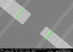
Bragg microcavity filter for optical sensingJames Dou |
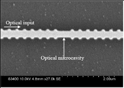
Optical microcavity filters play vital roles both in telecommunication and sensing applications. One very attractive optical microcavity is the bragg microcavity formed by a periodic dielectric slot waveguide. Strong light confinement in the low refractive index slot region formed by two silicon slabs on a silicon dioxide substrate makes this structure useful for optofluidic, sensing, and optical trapping applications. We have demonstrated that good sensitivity can be achieved using this structure. |
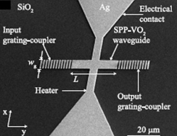
Lossy optical materials for absorption based switchingArash Joushaghani |
|
Optical
absorption is usually undesirable in photonic
integrated systems as it results in
attenuation of signal power. However, from a
design perspective, optical materials with
large absorption can be a powerful tool in
designing optical system. They not only allow
us to properly do impedance matching between
different photonic components, but also
enable efficient detectors and absorption
based switches. We are investigating novel
and lossy optical materials to demonstrate
optical switching. Emphasis is placed on
using Vanadium Dioxide (VO2) in a hybrid
plasmonic system to achieve optical
switching. |