
Research
My research is primarily on integrated micro- and nano-photonic devices in semiconductors. By miniaturizing and integrating several different types of optical components monolithically in photonic integrated circuits (PIC) on a single microchip, I aim to create devices that reduce cost, lower power consumption, increase performance, and improve robustness. In particular, I am involved with the following projects:
- High Capacity Transport PICs using GaAs and Vertical Integration
- Nonlinear PICs in GaAs/AlGaAs Superlattice
- Hybrid Plasmonic/Semiconductor Waveguides
High Capacity Transport PICs using GaAs and Vertical Integration
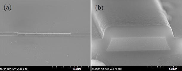
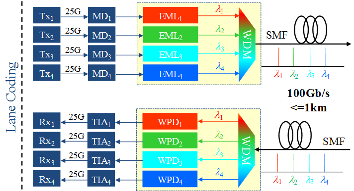 Interconnects in large data centres are largely being transitioned over to optical technology to keep up with the demand for high-bandwidth Internet-based services. However, the current optical transciever technology either does not provide adequate reach distance to cover the data centre warehouse or are too expensive to deploy on a massive scale. Part of the problem is that present transeivers are built with discrete components that are costly to assemble together. Another problem is the cost of the materials traditionally used for those components, i.e. InP. In our approach, we aim to reduce the overall cost of optical interconnect transceivers in two ways: 1) PIC technology using vertical integration, and 2) GaAs-based materials. Vertical integration is a compelling approach to optical integration since it avoids costly etch-and-regrowth processes commonly used in other PIC technologies. GaAs is significantly less expensive as a material and to process than InP. Links based on these PICs will operate in the 850 nm optical window over single-mode fibre. The PICs will contain several devices including wavelength division multiplexors, lasers, photodetectors, and spot-size converters. The system will be capable of supporting 100 Gbps links with potential increases in bit rate in the future.
This project is being done in collaboration with OneChip Photonics, Inc.
Nonlinear PICs in GaAs/AlGaAs Superlattice

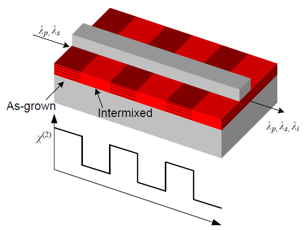 GaAs/AlGaAs superlattice is a nanostructured and highly nonlinear optical material with potential applications in all-optical signal processing. The ability to tune the bandgap and optical nonlinear properties by quantum well intermixing (QWI) postgrowth techniques make it attractive for fabricating complex structures and for monolithically integrating multiple devices into a single-chip PIC. In my research, I have shown that superlattices also have unique nonlinear optical properties which may be useful for a number of functions. In particular, we are designing new waveguide structures for highly-efficient quasi-phase-matched (QPM) optical three-wave mixing. We plan to integrate QPM waveguides with on-board pump lasers to form an tunable monolithic optical parametric oscillator (OPO) outputing wavelengths in the telecommunications and mid-infrared spectral bands. Such a disruptive technology would have many wide-reaching applications, and have cost, efficiency, and footprint advantages over current technologies. Potentially, a compact device based on a PIC could enable inexpensive optical communications devices for the telecom industry, and portable or in-situ spectroscopic devices for gas and chemical sensing applications.
Project team members: Peyman Sarrafi.
Hybrid Plasmonic/Semiconductor Waveguides
Plasmonic waveguides have demonstrated several interesting features such as the ability confine light into small volumes. However, they have traditionally been too lossy for many practical applications. Furthermore, the polarization sensitivity limits their use. Hybrid plasmonic/semiconductor waveguides are alternative types of optical waveguides that exhibit lower loss while providing high optical confinement. This opens up a number of applications for integrated optical devices. For instance, we have demonstrated very short on-chip polarizers that can be used for polarization control of light in PICs. The waveguides can be produced using inexpensive materials such as silicon-on-insulator and CMOS compatible fabrication methods.
Project team members: Mohammed Alam, Xiao Sun, Prof. Stewart Aitchison, and Prof. Mo Mojahedi.